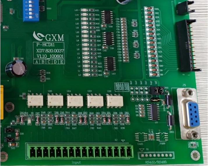
PCB Assembly lines quick turn prototype for SMT PCB Assembly
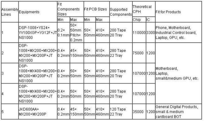
quick turn prototype & mass production for SMT PCB Assembly 6 PCB Assembly lines
Detail Specifications:
|
Layers
|
2
|
|
Material
|
FR-4
|
|
Board Thickness
|
1.6mm
|
|
Copper Thickness
|
1oz
|
|
Surface Treatment
|
HASL LF
|
|
Soldmask & Silkscreen
|
Green & White
|
|
Quality Standard
|
IPC Class 2, 100% E-testing
|
|
Certificates
|
TS16949, ISO9001, UL, RoHS
|
What we can do for you:
· PCB & PCBA Design
· PCB manufacturing (prototype, small to medium, mass production)
· Components Sourcing
· PCB Assembly/SMT/DIP
To get a full quotation of the PCB/PCBA, pls provide the information as below:
· Gerber File, with detail specification of the PCB
· BOM List (Better with excel fomart)
· Photoes of the PCBA (If you have done this PCBA before)
Manufacturer Capacity:
|
Capacity
|
Double Sided: 12000 sq.m / month
Multilayers: 8000sq.m / month
|
|
Min Line Width/Gap
|
4/4 mil (1mil=0.0254mm)
|
|
Board Thickness
|
0.3~4.0mm
|
|
Layers
|
1~20 layers
|
|
Material
|
FR-4, Aluminum, PI
|
|
Copper Thickness
|
0.5~4oz
|
|
Material Tg
|
Tg140~Tg170
|
|
Max PCB Size
|
600*1200mm
|
|
Min Hole Size
|
0.2mm (+/- 0.025)
|
|
Surface Treatment
|
HASL, ENIG, OSP
|
SMT Capacity

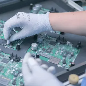
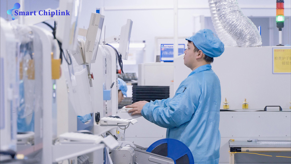
SMT (Surface Mount Technology) PCB assembly is a method of populating and soldering electronic components onto a printed circuit board (PCB). In SMT assembly, components are mounted directly onto the surface of the PCB rather than passing through holes as in through-hole assembly. SMT is widely used in modern electronics manufacturing due to its advantages in terms of component size, density, and automation. Here are the key steps involved in SMT PCB assembly:
Stencil Printing: The first step is to apply solder paste onto the PCB. A stencil, typically made of stainless steel, is aligned over the PCB, and solder paste is deposited through the openings in the stencil onto the solder pads. The solder paste contains tiny solder particles suspended in flux.
Component Placement: Once the solder paste is applied, an automated component placement machine, also known as a pick-and-place machine, is used to accurately position and place the SMT components onto the solder paste. The machine picks up the components from reels, trays, or tubes and precisely places them on the designated locations on the PCB.
Reflow Soldering: After component placement, the PCB with the solder paste and components goes through a reflow soldering process. The PCB is subjected to controlled heating in a reflow oven, where the solder paste undergoes a phase change from a paste to a molten state. The molten solder forms metallurgical bonds between the component leads and the PCB pads, creating reliable electrical and mechanical connections.
Inspection and Testing: Following the reflow soldering process, the assembled PCB is inspected and tested for quality assurance. Automated optical inspection (AOI) systems or other inspection methods are used to detect solder defects, such as insufficient or excessive solder, misaligned components, or solder bridges. Functional testing may also be performed to verify the functionality of the assembled PCB.
Additional Processing: Depending on the specific requirements of the PCB assembly, additional steps may be carried out, such as conformal coating application, cleaning, or rework/repair for any identified defects. These steps ensure the final quality and reliability of the SMT assembly.
SMT PCB assembly offers several advantages, including higher component density, reduced manufacturing costs, improved signal integrity, and increased production efficiency. It enables the assembly of smaller and lighter electronic devices with enhanced performance.
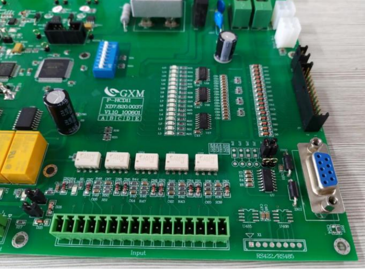
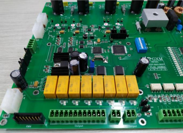
Photoes of this quick turn prototype & mass production for SMT PCB Assembly 6 PCB Assembly lines


 English
